
Key points
- Moving data between memory and processor costs more energy than the math itself. In-memory computing removes that trip.
- A memristor crossbar computes a full matrix-vector multiply in one analog step: Ohm's law multiplies, Kirchhoff's law adds.
- Precision was the hard problem. TetraMem's founders showed 2,048 distinct levels in one memristor cell (Nature, 2023).
- TetraMem's MLX200 brings multi-level RRAM in-memory computing to TSMC 22nm. First silicon was validated in May 2026.
01
The memory wall: why AI spends its energy moving data
Every neural network runs on one core operation, repeated billions of times: multiply each input by a weight, then add the results. In a conventional processor, the weights live in memory and the multipliers live in a separate compute unit. Each operation needs the weights to travel across a bus first.
That trip is the expensive part. Moving a number from memory costs far more energy and time than multiplying it, and models keep growing. In conventional AI hardware, up to 90% of the power goes to moving data rather than computing on it. Engineers call this the memory wall.
Conventional chip
In-memory computing
At the edge, the memory wall shows up as a drained battery, a warm device and a slow response. In-memory computing attacks the cause: it does the math where the weights already are.
02
How a memristor crossbar computes
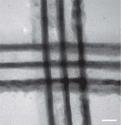
A crossbar is a grid of wires: rows run one way, columns the other, and a memristor sits at every crossing. Each memristor is a programmable resistor. Its conductance, how easily current flows through it, stores one weight of the model.
- Store
Program each memristor to a conductance level that represents one weight. RRAM keeps that value with the power off.
- Apply
Digital-to-analog converters (DACs) turn the input values into voltages on the rows.
- Multiply
Ohm’s law does the multiplication: the current through each cell equals its voltage times its conductance.
- Add
Kirchhoff’s current law does the addition: the currents on each column add up on the wire.
- Read
Analog-to-digital converters (ADCs) turn each column’s current into a digital value for the next layer.
The result is a full matrix-vector multiply in one step, with every column working at the same time. A 256×256 array, the size TetraMem’s founders reported in Nature, holds 65,536 weights and uses all of them in a single read.
03
Memristor vs RRAM: what the terms mean
- Memristor
- Short for “memory resistor”: a two-terminal device whose resistance depends on the current and voltage it has seen. Leon Chua described it in theory in 1971. HP Labs linked it to a real device in 2008, the research line TetraMem’s founders came from.
- RRAM
- Resistive random-access memory, also written ReRAM. A memory technology built from resistive-switching cells, usually a thin oxide between two electrodes. Like flash, it keeps data with the power off.
- Multi-level RRAM
- RRAM cells programmed to many distinct conductance levels instead of just on and off, so one cell holds a multi-bit weight. This is what TetraMem builds on.
- Compute-in-memory
- Another name for in-memory computing (CIM or IMC). It covers both digital and analog approaches.
04
Digital vs analog in-memory computing
Both approaches bring compute closer to memory. They differ in how the math is done. Digital in-memory computing adds digital logic inside or beside memory blocks. Analog in-memory computing lets the physics of the memory cells do the work.
| Property | Conventional processor | Digital in-memory | Analog in-memory (RRAM) |
|---|---|---|---|
| Where the math happens | Separate compute units, after weights are fetched from memory | Digital logic built into or beside memory arrays (often SRAM) | Inside the memory array, by the physics of the cells |
| How a multiply-add works | Digital multipliers and adders, one operation at a time per unit | Digital adders next to each memory block | Ohm's law multiplies, Kirchhoff's law adds, a whole column at once |
| Weight movement | Weights move for every operation | Short moves inside the memory block | Weights stay in place |
| Weights at power-off | Reloaded from external memory | Lost with SRAM; reloaded at start-up | Kept, because RRAM is non-volatile |
| Main engineering challenge | Memory bandwidth and energy per byte moved | Area and capacity of on-chip memory | Precision, noise and data conversion at the array edges |
05
Why precision was the hard part, and how multi-level cells solve it
Analog values are never perfectly exact. Early memristors held only a handful of reliable states, and noise between levels limited how precisely a weight could be stored. For years that was the main argument against analog AI chips.
distinct conductance levels in a single memristor, integrated on CMOS and built in a commercial foundry. That is 11 bits per cell. Nature, 2023
In 2023, TetraMem’s founders and their university partners reported thousands of conductance levels in memristors on CMOS. The key was learning how to program each cell precisely and settle it at its target level.
In 2024, a paper in Science went further: a method to program memristor arrays with arbitrarily high precision for analog computing. It spreads one high-precision number across several arrays, each one correcting the error left by the one before, so precision can rise as far as a task needs.
06
Where analog in-memory computing matters
The gains count most where power is scarce and AI has to run all the time. That is the edge: devices on a small battery that must answer at once, without a trip to the cloud.
- Hearables and audio. Always-on voice and audio processing in earbuds and headsets.
- Wearables and health. Continuous monitoring, processed on the wrist.
- AR and VR. Low-latency vision and sensing in headsets and smart glasses.
- Smart sensors and IoT. Sensors that decide locally, so only results leave the device.
- Edge to cloud. The same approach scales to chiplets for data-center inference, where power is now the limit.
See the full list on the applications section of the homepage.
07
How TetraMem builds it
TetraMem was founded in 2018 by researchers from HP Labs, USC and UMass Amherst. Its chips put multi-level RRAM arrays at the center of the design.
MLX200
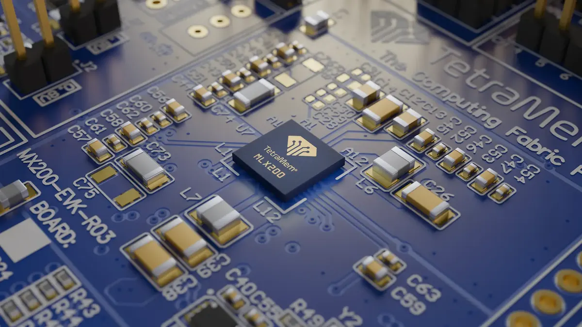
The first multi‑level RRAM in‑memory computing chip on 22nm
- TSMC 22nm process
- RRAM compute arrays with mixed-signal compute engines
- Andes NX27V RISC-V vector CPU
- ONNX models in, INT8 and INT4 quantization
- Silicon validated May 2026. Evaluation kits in the second half of 2026
08
Frequently asked questions
What is in-memory computing?
In-memory computing, also called compute-in-memory, is a chip design where calculations happen inside or next to the memory that holds the data, instead of in a separate processor. It cuts the energy and time spent moving data, which dominates the cost of running AI models.
What is the difference between analog and digital in-memory computing?
Digital in-memory computing places digital logic inside or beside memory arrays and adds numbers bit by bit. Analog in-memory computing uses the physics of the memory cells: stored conductance and applied voltages produce currents that multiply and sum in one step across a whole array.
What is the difference between a memristor and RRAM?
A memristor is a two-terminal device whose resistance depends on the electrical history it has seen. RRAM, or resistive random-access memory, is a memory technology built from such resistive-switching cells. In practice the terms often describe the same device: TetraMem's cells are multi-level RRAM memristors.
Why does analog in-memory computing save power?
In conventional AI hardware, most of the energy goes to moving weights between memory and compute, not to the arithmetic. Analog in-memory computing keeps the weights in place and does the multiply-and-add inside the array, so that traffic disappears.
Is analog computing accurate enough for AI?
Yes, when the cells hold enough distinct levels and can be programmed precisely. TetraMem's founders showed 2,048 conductance levels in a single memristor integrated on CMOS (Nature, 2023), and a method to program memristor arrays to arbitrarily high precision (Science, 2024).
What AI models can run on TetraMem chips?
TetraMem's compiler takes models in the ONNX format, quantizes them to INT8 or INT4, and produces C++ and RISC-V executables. Published work on TetraMem silicon covers neural-network inference and real-time signal processing, including radio-frequency signals.
What is MLX200?
MLX200 is TetraMem's multi-level RRAM analog in-memory computing system-on-chip, built on TSMC 22nm. It pairs RRAM compute arrays with mixed-signal compute engines and an Andes NX27V RISC-V vector CPU. First silicon was validated in May 2026.
When can I evaluate MLX200?
TetraMem plans MLX200 evaluation kits for the second half of 2026. You can request one from the TetraMem team today.
Sources
- Nature, 2023Thousands of conductance levels in memristors integrated on CMOS
- Science, 2024Programming memristor arrays with arbitrarily high precision for analog computing
- Nature Electronics, 2025Radiofrequency signal processing with a memristive system-on-a-chip
- Science Advances, 2025Real-time signal processing enabled by fused networks on a memristor-based system on a chip
- Science, 2026High-temperature memristors enabled by interfacial engineering
- TetraMem, May 2026TetraMem completes MLX200 silicon validation